

On 18 November 2026, Architect Labs disclosed Frostbite, a general-purpose CPU design that it says reached final GDS at 7 nm and delivered 4.59× the performance per watt of an undisclosed dual-issue, in-order CPU across 25 workloads. Frostbite is a finished pre-silicon design, not a purchasable processor or a tapeout announcement.
At a glance
- Architect Labs reports Frostbite reached 500 MHz in final GDS after meeting 800 MHz timing at synthesis.
- Its headline 4.59× performance-per-watt result combines 10 workloads used for tuning with 15 held-out workloads.
- The held-out set achieved 3.83× the comparison CPU’s performance per watt, according to Architect Labs.
- A Frostbite quad plus four L3 memory nodes occupies 0.792 mm², against 0.895 mm² for the disclosed comparison core.
- The company says it plans an FPGA playground, an operating system, and later RTL and ISA releases, but gives no dates.
Is Frostbite a CPU?
Frostbite is a CPU architecture, not the Frostbite game engine, a graphics API, or CPU cooling paste. Architect Labs calls it a general-purpose processor with a new instruction set architecture, or ISA: the rules that define what software asks the chip to do. Its programs are written in Vine and compiled into an interaction-net representation called Ivy.
The important distinction is that Frostbite does not start from the usual stream of instructions and then search for independent work. It begins with a graph that records dependencies. The chip is designed to execute graph rewrites where the dependencies permit them. Architect Labs says that choice lets the hardware distribute work over a mesh of tiles rather than depend on a large central scheduler. The company’s architecture description is the only public technical account of the processor so far.
Vine is presented as a Rust-like language that compiles directly to interaction nets. The public Vine site identifies it simply as The Vine Programming Language; it does not yet publish a Frostbite compiler release or a supported hardware target. That matters because the software toolchain is part of the claimed architecture, not an optional layer added later.
How does Frostbite CPU architecture work?
Frostbite CPU architecture works by preserving three properties in the program graph: local computation, explicit dependencies, and single ownership of values. An interaction net consists of nodes linked by ports. A pair connected at their principal ports can be rewritten locally, and independent pairs can run in parallel. Tendrils’ explanation of interaction nets describes why non-overlapping active pairs can execute in any order without changing the result.
That model changes what the chip must manage. Conventional CPUs commonly spend hardware effort predicting branches, issuing instructions out of order, and keeping several cache levels coherent. Frostbite instead aims to keep data close to its owner and preserve dependencies from compiler output to execution. This does not remove the need for communication; it moves more of the work into local memories and an on-chip network.
Architect Labs describes the unit of execution as a short section of code that runs when its inputs are ready. If a branch or loop produces an unknown number of tasks, the running tile stores the continuation in a local “frame manager,” places new tasks in a work queue, then continues with the newest one. Empty neighboring tiles may pull queued work through the network. When all required return packets arrive, a counter wakes the parked continuation. The published tile description calls this distributed work stealing.
In plain English, Frostbite tries to make parallel work visible early and keep it visible. The claimed gain is not that it makes one instruction faster. It is that a recursive search, a branch-heavy parser, or a parallel kernel can spread work across tiles without a programmer manually constructing threads, locks, and shared queues.
Was Frostbite designed by AI
Architect Labs says AI agents explored and revised Frostbite’s compiler, ISA, architecture, microarchitecture, RTL, verification, and final layout together. RTL, or register-transfer-level code, is the hardware description used to define digital logic before a chip layout is produced. The company says agents first narrowed candidate architectures with Python models, then generated an initial RTL design.
The first exploration produced a 141-page architecture proposal, according to Architect Labs. The company says it deleted that proposal after the first RTL iteration because estimated figures were not physically realistic enough. That is a useful detail: the process did not treat an AI-produced architecture narrative as the durable source of truth. It replaced it with formal contracts and calibrated models. Architect Labs’ process account says the agents explored 58 ideas over four searches and a final ablation round, retaining 37.
This is more ambitious than a model editing a multiplier or pipeline stage. OpenAI’s 18 November 2026 chip-design account describes models rewriting RTL and checking candidate changes with established design tools. It also warns that written requirements can let models omit features that do not help a narrow throughput score. OpenAI’s evaluation notes say tighter area limits, fuller feature requirements, and timing after physical synthesis would make CPU-design tests more representative.
Frostbite’s reported approach attempts to reduce that gap by treating the compiler, hardware, and evaluation workloads as one loop. It should not be read as evidence that AI independently discovered every concept. Interaction nets predate Frostbite by decades. The AI claim is that agents selected, combined, implemented, and optimized this architecture through the full pre-silicon flow.
How was Frostbite verified?
Frostbite was verified against an in-house formal specification language called ASL, according to Architect Labs. ASL is said to translate and refine across system models, RTL, UVM testbenches, SystemVerilog assertions, and other implementation forms. UVM is a standard simulation testbench method; an assertion is a machine-checkable statement that a design must always satisfy.
The company says ASL translated to more than 800,000 lines of Lean, a theorem-proving system used to check mathematical claims about a program or circuit. The Lean 4 paper describes Lean as an extensible interactive theorem prover and programming language. Frostbite’s public account does not release its ASL contracts, Lean files, RTL, testbenches, proof logs, or the exact tool commands used to run them.
That limitation matters because a passing simulation suite does not prove a specification was complete. A paper submitted on 19 November 2026 found that conventional UVM scoreboards can miss “scoreboard escapes”: exercised bugs that pass tests yet violate the specification. The researchers inserted 564 bugs into four OpenTitan IP blocks and confirmed 41 such escapes. The paper’s abstract supports the general verification caution, but it did not test Frostbite.
Architect Labs’ core claim is stronger than “the tests passed.” It says each proposed revision was checked against ASL contracts, modeled in Arcmodel, implemented in RTL, and measured for power before being kept or dropped. That is a credible structure for catching inconsistency between layers. It is not equivalent to public reproducibility until external engineers can inspect the contracts, generated RTL, proof obligations, test the public record, and outcomes.
How fast is Frostbite CPU?
Frostbite reached 800 MHz timing at synthesis and 500 MHz in final GDS, Architect Labs says. GDS is the layout database sent toward chip manufacturing; it is not proof that physical chips have been fabricated or measured. The disclosed comparison pairs one Frostbite quad, a two-by-two tile grid plus four L3 nodes, with a single unnamed dual-issue in-order CPU core at the same 7 nm process.
The public performance claim is therefore best read as a pre-silicon, workload-specific efficiency comparison. Architect Labs reports that Frostbite’s cluster occupies 0.792 mm² while its comparison CPU uses 0.895 mm². It also says the exact competitor core cannot be disclosed for legal reasons. The results section does not publish absolute throughput, wattage, clock conditions for the comparison core, compiler flags, memory configuration, or per-workload runtimes.
| Workload cohort | Number of workloads | Performance per watt versus TCPU | What it shows |
|---|---|---|---|
| Search set | 10 | 6.02× | Programs used while the architecture was optimized. |
| Held-out evaluation set | 15 | 3.83× | Programs withheld until final evaluation. |
| Combined result | 25 | 4.59× | The headline geometric mean, mixing tuned and held-out work. |
Source: Architect Labs’ Frostbite benchmark disclosure. “Geometric mean” reduces the effect of one unusually large result, but it does not replace per-workload data.
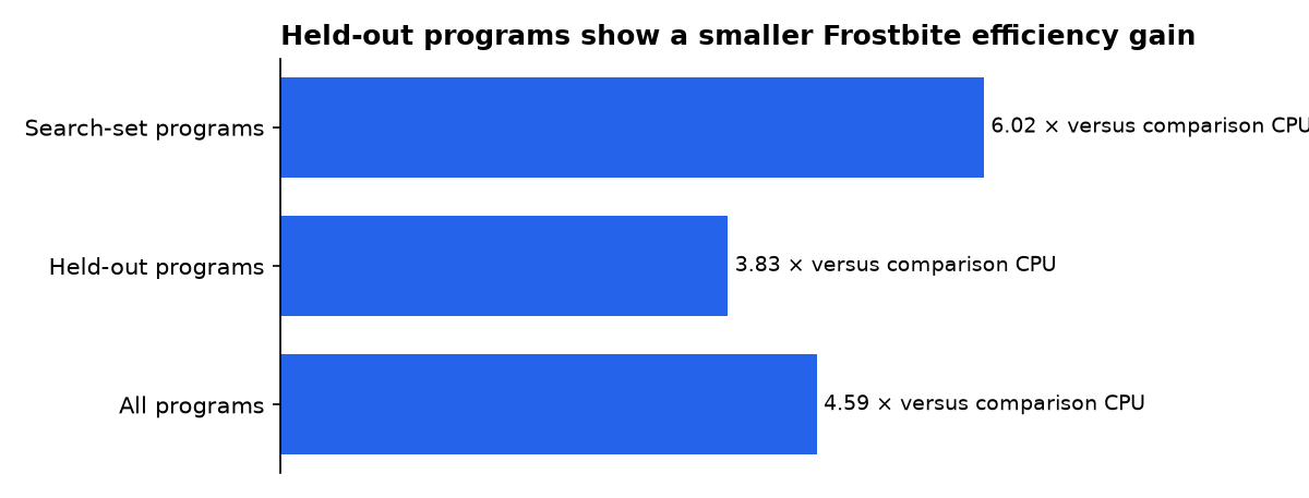
The difference between 6.02× on the search set and 3.83× on the held-out set is the most informative published result. It suggests the architecture retained a large claimed advantage outside its tuning suite, while also showing that the headline figure benefits from workloads used during optimization. Architect Labs reports 8.77× performance per area across all workloads, but its disclosed data still cannot establish how Frostbite compares with an out-of-order desktop core, a server CPU, or a modern mobile CPU.
The workload suite includes dense kernels such as matrix multiplication and convolution, plus branching and recursive programs including JSON parsing, Huffman coding, k-d trees, and Fibonacci. The FFT, radixsort, and LU kernels followed SPLASH-2 implementations but were made 64 times smaller for exploration. The cited SPLASH-2 repository is a modified pthreads implementation; its last public commit dates to 21 April 2013, so it is a code source rather than evidence of Frostbite’s performance.
What was promised versus what shipped?
Frostbite’s current status is clear on one point: Architect Labs says it completed a final GDS layout. It has not announced a tapeout, manufactured chips, external benchmark replication, or a public SDK. The timeline separates completed pre-silicon artifacts from work the company says it intends to release.
| Date | Claim or commitment | Status disclosed publicly |
|---|---|---|
| 27 August 2026 | Architect Labs said its Redwood accelerator would continue toward full GDSII and a TSMC tapeout. | Redwood was described as an FPGA deployment with ASIC projections, not manufactured ASIC silicon. |
| 18 November 2026 | Architect Labs introduced Frostbite as an AI-designed and AI-verified CPU architecture. | The company said the project had reached final GDS at 7 nm. |
| 18 November 2026 | Frostbite was benchmarked against an unnamed 7 nm in-order CPU core. | Architect Labs published relative pre-silicon results across 25 workloads. |
| No date announced | Provide an FPGA-hosted software playground. | Planned; no public availability date. |
| No date announced | Release Frostbite RTL and ISA, and expand testing to SPEC and PARSEC. | Planned; no public code, benchmark package, or schedule. |
Sources: Architect Labs’ Redwood announcement and the Frostbite roadmap.
The timeline also explains why Frostbite should not yet be compared with a retail processor. Final GDS means the design has completed a layout stage. It does not provide measured frequency yield, leakage, thermal behavior, memory-system behavior under board-level conditions, or silicon power. Those are the numbers that decide whether a pre-silicon performance-per-watt estimate survives contact with a fabricated chip.
Can you use Frostbite today?
No public Frostbite processor, FPGA image, compiler package, ISA manual, RTL repository, or benchmark harness was available in the announcement. Architect Labs says it intends to host a software playground on FPGAs, develop an operating system with virtualisation support, test more CPU configurations, and release the RTL and ISA. It supplied no launch dates for those items.
That makes Frostbite a research and design-flow result today, rather than a platform developers can evaluate. Developers cannot yet compile a known Vine program, inspect generated Ivy, reproduce the 25-workload suite, or measure a board. The company’s promise to release the ISA and RTL is therefore central: it would let independent teams check whether the architecture’s claimed advantages come from the interaction-net model, particular workloads, physical-design choices, or the undisclosed comparison baseline.
What we could not verify?
Frostbite’s exact ISA, RTL, ASL contracts, Lean proofs, compiler version, benchmark sources, test inputs, comparison CPU identity, power methodology, and absolute performance results are not public. No independent laboratory has reported measurements from manufactured Frostbite silicon, and no tapeout date has been announced.
Architect Labs could settle most of those questions by releasing the promised RTL, ISA, reproducible benchmark harness, synthesis constraints, power assumptions, and proof artifacts. A fabricated chip measured by an independent lab could settle the remaining questions about frequency, energy, thermals, and whether Frostbite’s pre-silicon advantage survives production conditions.
Sources
- Architect Labs — Introducing Frostbite: A new CPU architecture discovered, designed, and verified end-to-end by AI
- Tendrils — On Interaction Nets
- Vine — The Vine Programming Language
- Springer — The Lean 4 Theorem Prover and Programming Language
- arXiv — Verify the Verifier: Specification-Grounded LLM Cross-Checking for Bugs That Escape UVM Scoreboards
- OpenAI — Advancing chip design with OpenAI models
- GitHub — liuyix/splash2_benchmark
- Architect Labs — Introducing Redwood

